Introduction
Brandon's semiconductor simulator (SemiSim) is an educational tool made with the original purpose of helping its creator understand semiconductor devices. It is fully interactive, letting users draw circuits and create their own devices in a manner similar to painting software. There is a wide variety of different materials to choose from and many ways to visualize the electromagnetic phenomena associated with semiconductors. Users can either load one of the many premade simulations or create their own.Physics
The simulation is set on a two-dimensional grid over which it solves the 2D Maxwell equations. The electric field lies in the same plane as the surface of the screen whereas the magnetic field is perpendicular to it. On top of this, there are two types of charge carriers, electrons and holes, which feel electric and chemical forces that determine their dynamics. The simulation uses a FDTD (finite-difference time domain) scheme obtained by discretizing the Maxwell equations and the drift-diffusion equations and coupling the two together. This results in a simulation that demonstrates many of the important properties of semiconductors and semiconductor devices, such as:- PN junctions
- Metal-semiconductor junctions
- Field effect transistors
- Galvani potential
- Thermoelectricity
Limitations
Because the simulation uses a very simplified model of how semiconductors work, it is not able capture some phenomena that show up in real systems. Things that the simulation cannot handle include:- Metal band structures
- Electrical breakdown
- Kinetic effects
- Quantum tunelling
- Velocity saturation
- Fermi level pinning
- Different recombination mechanisms
Simulation features
The interface consists of the simulation area which the user can interact with and the settings panel containing all the simulation controls.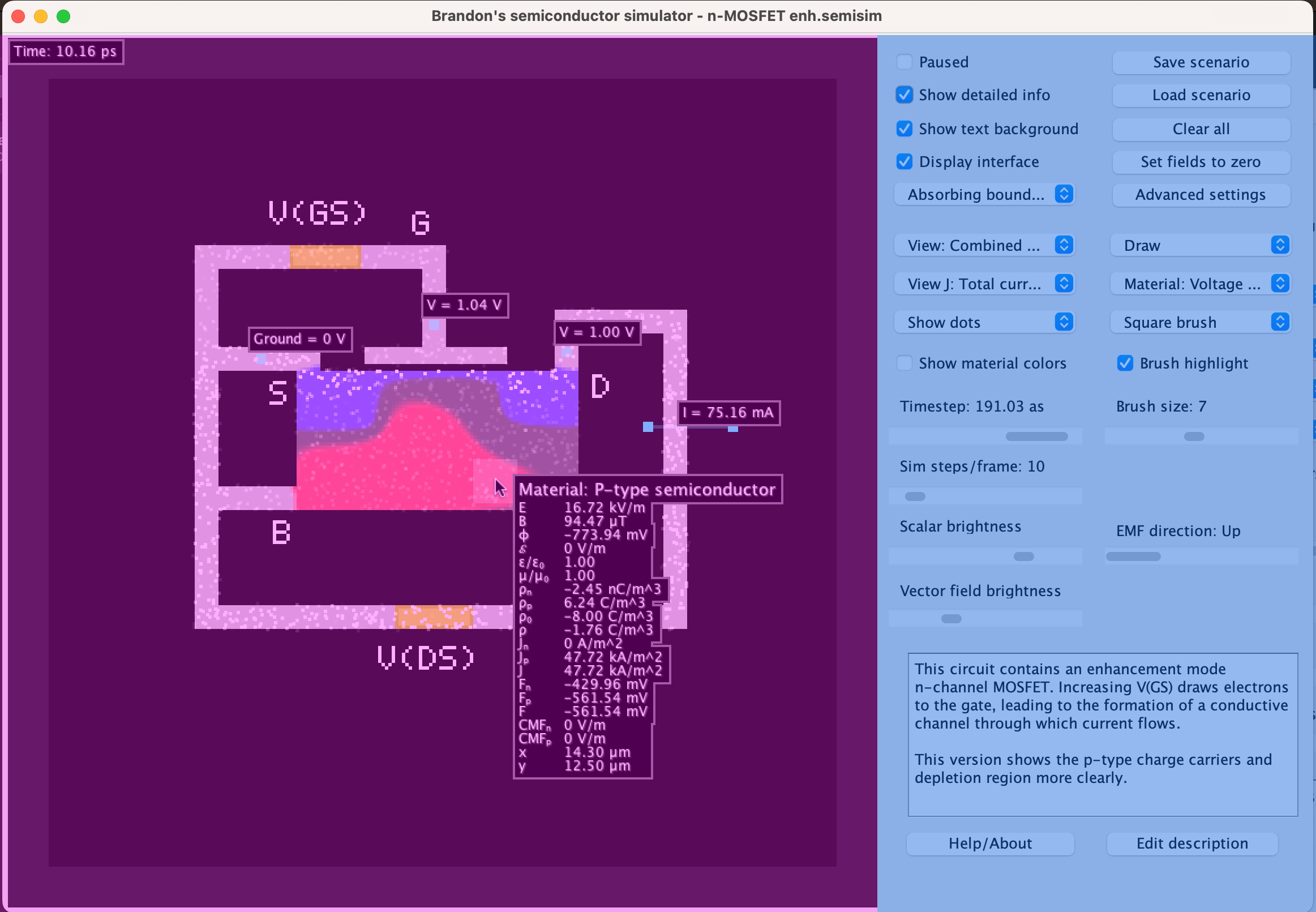
Simulation variables
Listed below are the most important variables that capture the state of the simulation at a given time:| \(\vec{E} = (E_x, E_y, 0)\) | Electric field [V/m] |
| \(\vec{B} = (0, 0, B_z)\) | Magnetic field [T] |
| \(\rho_n\) | Charge density of electrons [C/m^3] |
| \(\rho_p\) | Charge density of holes [C/m^3] |
| \(\rho = \rho_n + \rho_p\) | Net charge density [C/m^3] |
| \(\vec{J}_n = (J_{nx}, J_{ny}, 0)\) | Electron current density [A/m^2] |
| \(\vec{J}_p = (J_{px}, J_{py}, 0)\) | Hole current density [A/m^2] |
| \(\vec{J} = \vec{J}_n + \vec{J}_p\) | Total current density [A/m^2] |
| \(\vec{D} = \epsilon \vec{E}\) | Electric displacement field [C/m^2] |
| \(\vec{H} = \frac{1}{\mu} \vec{B}\) | Magnetic field [A/m] |
| \(\vec{S} = \vec{E}\times \vec{H}\) | Poynting vector [W/m^2] |
| \(u = \frac{1}{2}(\vec{E}\cdot \vec{D} + \vec{B} \cdot \vec{H})\) | Electromagnetic energy density [J/m^3] |
| \(\phi\) | Electric scalar potential [V] |
| \(G\) | Charge carrier generation rate [1/(m^3 s)] |
| \(R\) | Charge carrier recombination rate [1/(m^3 s)] |
| \(F_n\) | Electron quasi-Fermi level (free energy) [V]* |
| \(F_p\) | Hole quasi-Fermi level (free energy) [V]* |
| \(F\) | Average free energy [V] |
| \(Q\) | Heat dissipation [J/(s m^3)] |
| \(S\) | Entropy generation [J/ (K s m^3)] |
Vector view modes
Arrows: The direction and brightness of arrows corresponds to the direction and magnitude of the vector field. 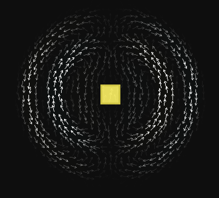
Lines:
The brightness and density of lines indicates the magnitude of the field. 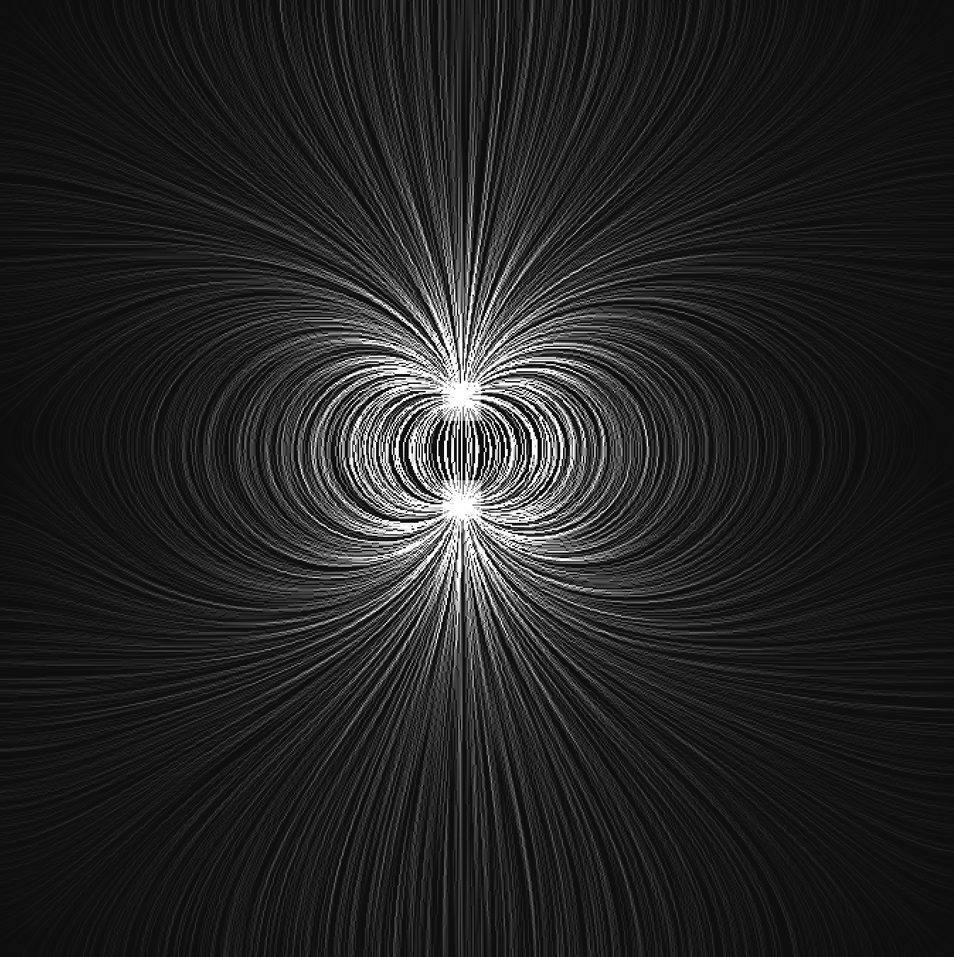
Dots [desktop]: The velocity of the dots is proportional to the value of the vector field. 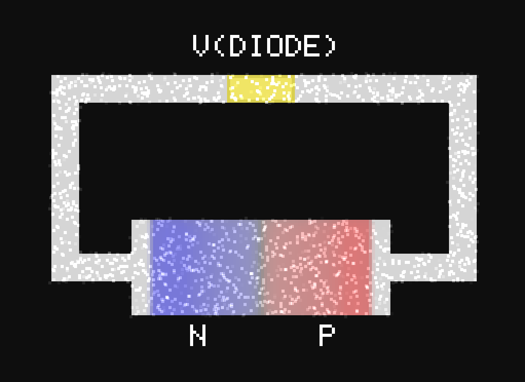
Contour [desktop]: Contour lines indicate a region on which the scalar field has a constant value. 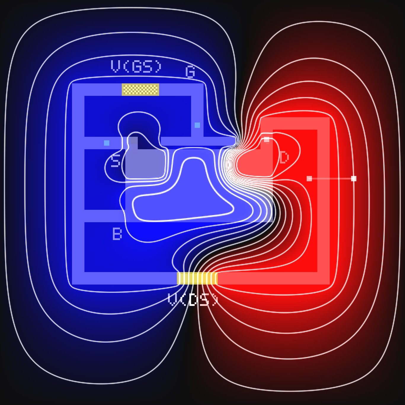
Charge carriers [desktop]: Electrons and holes are represented as blue and red dots, respectively.
Both dots move at the actual drift velocities of their corresponding charge carriers and their density accurately reflects the density of charge carriers. This is much more realistic but less flexible than the dots view. 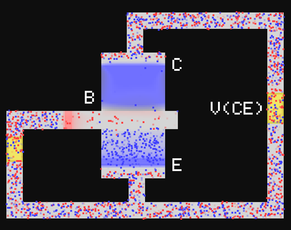
Options
| Pause | Pauses and unpauses the simulation. |
| Show detailed info | Displays a tooltip that contains the values of all the simulation variables at the cursor's location. |
| Show text background | Gives text boxes a black background, making the text easier to see. |
| Display interface | Shows probe info, graph locations, time, and tooltip. |
| Boundary condition | Choose between a boundary that absorbs outgoing radiation or a perfectly conductive boundary that reflects it. |
| Scalar view | Choose which field to display as a color scale over the simulation field. |
| Vector view | Choose which vector field to visualize (only works for 2D vectors, see "Vector view modes"). |
| Show material colors | If checked, gives each material a different color, making them easier to tell apart. |
| Timestep | Sets the simulation timestep. The maximum timestep is determined by the CFL condition for the wave equation and diffusion equations for each charge carrier. |
| Sim steps/frame | Sets the number of iterations performed during each frame. Most of the examples require at least 10 steps/frame to run responsively. The maximum number depends on how good the user's computer is. |
| Scalar brightness | Sets the brightness of the scalar field. |
| Vector brightness | Sets the brightness of the vector field. |
| Save scenario | Saves the current simulation to a file. |
| Load scenario | Loads a simulation from a file. SemiSim comes with a variety of pre-made simulations located in the "examples" folder. |
| Clear all | Removes all materials and resets all fields. |
| Set fields to zero | Sets all fields to their default values, leaving the materials unchanged. |
| Advanced settings [desktop] | Opens advanced simulation settings window, for advanced users only. |
| Tool | Selects one of the tools. |
Tools
| Interact | Allows user to control voltage sources and turn switches on and off by clicking. |
| Draw | Adds material to the field. |
| Voltage | Adds a voltage probe that measures electrochemical potential at a certain point (See "What do voltmeters actually measure"). |
| Current [click and drag] | Adds a current probe that measures current across a wire. |
| Ground | Specifies the point relative to which probes measure voltage (optional). |
| Delete probe | Click to delete a probe. |
| Plot bands [click and drag, desktop] | Specifies a 1D line along which the bands are plotted.
The plot contains the conduction and valence energy band edges as well as the quasi-Fermi levels of electrons in both bands. 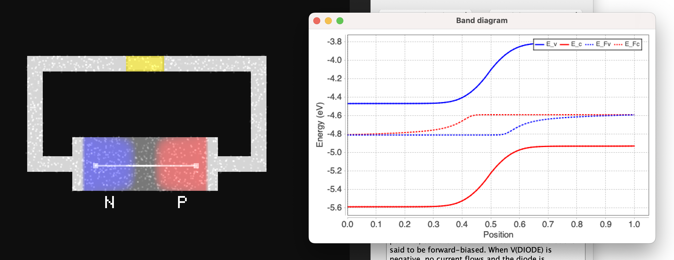 |
| Plot scalar field [click and drag, desktop] | Makes a plot of the currently selected scalar field. |
| Plot carriers [click and drag, desktop] | Makes a logarithmic plot of the number density of electrons and holes. |
| Flashlight [click and hold, desktop] | Shines a light on the region under the cursor. Light generates electron and hole pairs. |
| Replace | Similar to the draw tool, but overwrites occupied areas. |
| Line [click and drag] | Draws a line of material. |
| Fill | Fills a region with a certain material, similar to the bucket tool. |
| Erase | Erases material. |
| Select | Makes a rectangular selection which can be dragged around and moved. |
| Select region | Selects a contiguous region, similar to the bucket tool. |
| Text | Place a text cursor allowing text to be typed on the screen. |
Keyboard/Mouse Controls
| P or Space | Pause & unpause |
| F | Advance frame |
| Q | Change brush shape |
| C | Toggle material color |
| V | Toggle vectors |
| S | Toggle scalar colors |
| T | Toggle tooltip |
| G | Toggle text background |
| H | Toggle user interface |
| Mouse wheel | Change brush size |
| Shift | Draw straight lines |
| Ctrl | Fill area |
| Alt or Option | Pick material |
| Ctrl-X | Cut |
| Ctrl-C | Copy |
| Ctrl-V | Paste |
| Left mouse | Draw material |
| Right mouse | Erase material |
| Middle mouse | Pick material |
| R [desktop] | Record probe data (saves to probedata.txt) |
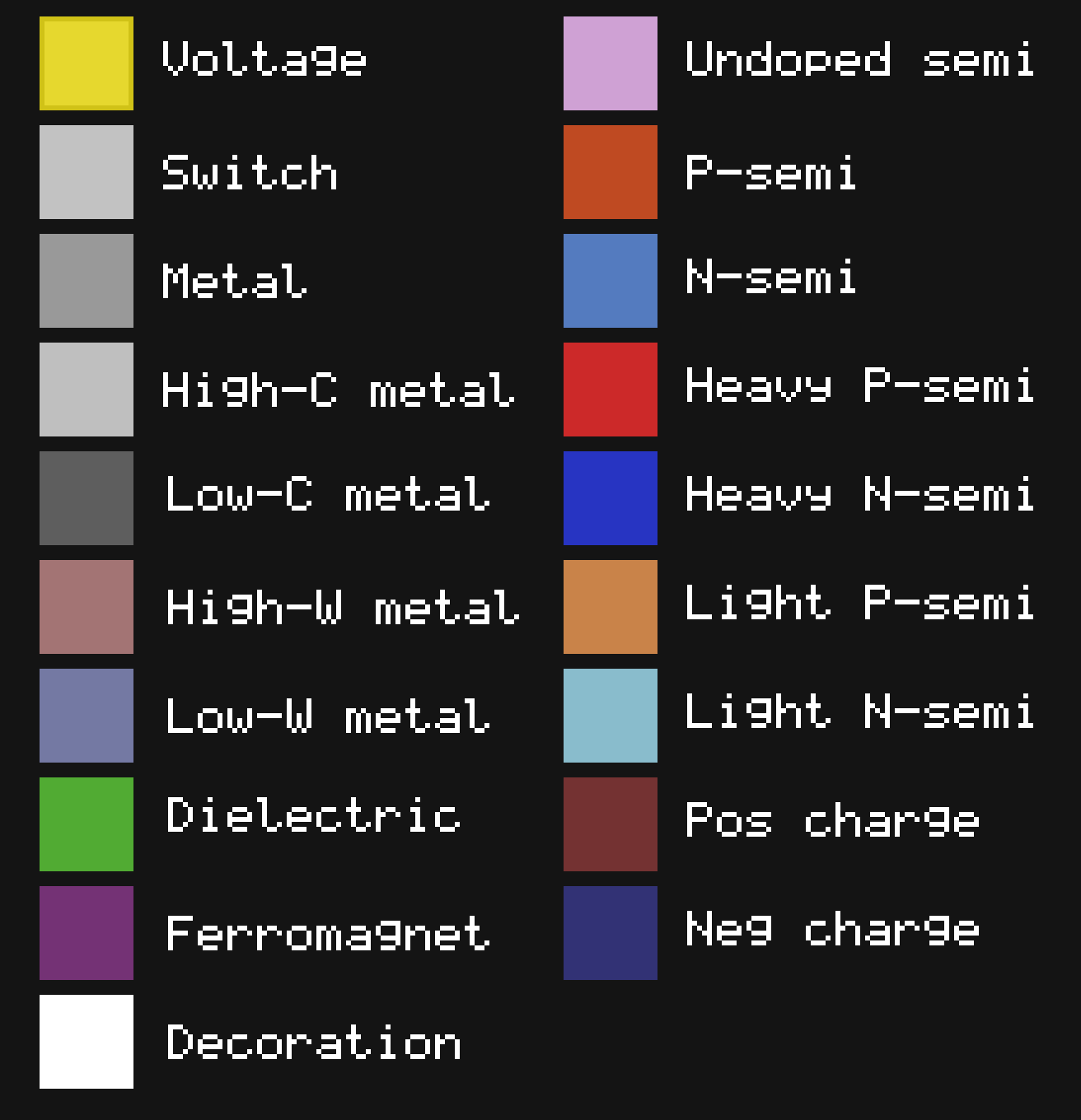
Materials
| Voltage source | Generates a voltage that can be used to power circuits. |
| Switch | Conductivity can be switched on and off by the user. |
| Metal | Material that conducts electricity very well. |
| Conductive metal | More conductive than regular metal. |
| Resistive metal | Less conductive than regular metal. |
| High workfunction metal | Metal that forms an ohmic contact with p-type semiconductor. |
| Low workfunction metal | Metal that forms an ohmic contact with n-type semiconductor. |
| Intrinsic semiconductor | Undoped, with equal number of electrons and holes. |
| P-type semiconductor | Represents a semiconductor doped with holes. |
| N-type semiconductor | Represents a semiconductor doped with electrons. |
| Heavily doped P-type semiconductor | Has a large concentration of holes. |
| Heavily doped N-type semiconductor | Has a large concentration of electrons. |
| Lightly doped P-type semiconductor | Has a small concentration of holes. |
| Lightly doped N-type semiconductor | Has a small concentration of electrons. |
| Dielectric | Material with a large permittivity/dielectric constant. |
| Ferromagnet | Magnetic material with high relative permeability. |
| Positive static charge | Positively charged insulating material. |
| Negative static charge | Negatively charged insulating material. |
| Decoration | Used for text or circuit symbols, has no effect otherwise. |
| Vacuum | Empty space. |
Miscellaneous questions and answers
Why does this simulation exist?
I created this simulator because I wanted to get a deeper understanding of how semiconductors work. It's been my experience that there's been a lack of good simulations that demonstrate advanced topics in physics. There certaintly exists many educational physics simulations, but they're all either aimed at lower educational levels, or they are very restricted in how the user can interact with the system. The only examples I've seen of simulations that combine advanced topics with a generous amount of interactivity are the physics applets written by Paul Falstad, to whom I'm also grateful for looking over my project and helping to convert it to Javascript. I've tried to give users many different ways of interacting with the simulation. Circuits can be drawn with just a few clicks of the mouse, allowing users to easily experiment with their own circuits. There are also many different ways of visualizing the underlying physics that I've incorporated into the settings. Each one gives a different perspective on the physics that is happening.What do the colors mean?
In general, the color red is associated with either holes or a positive charge. Blue represents electrons or negative charge. White means both electrons and holes exist a location. In the rest of the cases, yellow represents a positve quantity (eg. chemical potential or magnetic field), while cyan is negative. Finally, green is used for quantites that are always positive (eg. energy density). Note: Each material also has its own color which is unrelated to the aforementioned color scheme.What do voltmeters actually measure?
You might notice that the reading from a voltage probe doesn't match the electric potential Φ. In reality, voltmeters do not measure Φ but rather differences in electrochemical potential of charge carriers. Things get a bit trickier when we ask what the voltage is in a piece of semiconductor, becuase now there are multiple charge carriers! In this case we can try to define voltage as the reading we get when we stick a small metallic probe at a certain point. This can actually be performed in the simulation, and the result is that the electrochemical potential of the metal lies between that of electrons and holes, closer to whichever one has a larger density. I approximate this with a simple weighted average, the result of which is displayed on the voltage probe.Why does the magnetic field vanish outside of circuits?
Because the simulation is in 2D, circuits actually extend infinitely in the z-direction (out of the page), so current flowing through a closed circuit has the same effect as current flowing through a 3D solenoid. If you recall from E&M class, the magnetic field within an infinitely long solenoid is entirely contained within it. This is certainly a point of departure from how we expect circuits to behave. It means that each current loop has its own inductance, and trying to create "inductors" that behave like their 3D counterparts is quite tricky.
Copyright (c) 2025 Brandon Li
[email protected]